- 您现在的位置:买卖IC网 > Sheet目录368 > W631GG6KB-15 (Winbond Electronics)IC DDR3 SDRAM 1GBIT 96WBGA
�� �
�
�W631GG6KB�
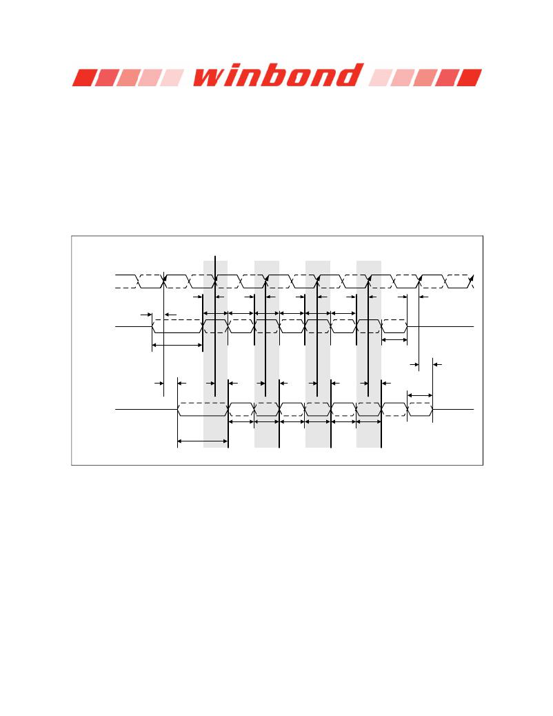
�8.13.2.1� READ� Timing;� Clock� to� Data� Strobe� relationship�
�Clock� to� Data� Strobe� relationship� is� shown� in� Figure� 24� and� is� applied� when� the� DLL� is� enabled� and�
�locked.�
�Rising� data� strobe� edge� parameters:�
�?�
�?�
�?�
�t� DQSCK� min/max� describes� the� allowed� range� for� a� rising� data� strobe� edge� relative� to� CK,� CK#.�
�t� DQSCK� is� the� actual� position� of� a� rising� strobe� edge� relative� to� CK,� CK#.�
�t� QSH� describes� the� data� strobe� high� pulse� width.�
�Falling� data� strobe� edge� parameters:�
�?�
�t� QSL� describes� the� data� strobe� low� pulse� width.�
�t� LZ(DQS)� ,� t� HZ(DQS)� for� preamble/postamble� (see� section� 8.13.2.3� and� Figure� 26).�
�RL� Measured�
�to� this� point�
�CK/CK#�
�t� DQSCK� (min)�
�t� DQSCK� (min)�
�t� DQSCK� (min)�
�t� DQSCK� (min)�
�t� HZ(DQS)� min�
�t� LZ(DQS)� min�
�t� QSH�
�t� QSL�
�t� QSH�
�t� QSL�
�t� QSH�
�t� QSL�
�DQS,� DQS#�
�Erly� Strobe�
�t� RPRE�
�t� RPST�
�Bit� 0�
�Bit� 1�
�Bit� 2�
�Bit� 3�
�Bit� 4�
�Bit� 5�
�Bit� 6�
�Bit� 7�
�t� HZ(DQS)� max�
�t� DQSCK� (max)�
�t� DQSCK� (max)�
�t� DQSCK� (max)�
�t� DQSCK� (max)�
�t� LZ(DQS)� max�
�t� RPST�
�DQS,� DQS#�
�Late� Strobe�
�t� QSH�
�t� QSL�
�t� QSH�
�t� QSL�
�t� QSH�
�t� QSL�
�t� RPRE�
�Bit� 0�
�Bit� 1�
�Bit� 2�
�Bit� 3�
�Bit� 4�
�Bit� 5�
�Bit� 6�
�Bit� 7�
�Notes:�
�1.� Within� a� burst,� rising� strobe� edge� is� not� necessarily� fixed� to� be� always� at� t� DQSCK� (min)� or� t� DQSCK� (max).� Instead,� rising� strobe�
�edge� can� vary� between� t� DQSCK� (min)� and� t� DQSCK� (max).�
�2.� Not� with� standing� note� 1,� a� rising� strobe� edge� with� t� DQSCK� (max)� at� T(n)� can� not� be� immediately� followed� by� a� rising� strobe�
�edge� with� t� DQSCK� (min)� at� T(n+1).� This� is� because� other� timing� relationships� (t� QSH� ,� t� QSL� )� exist:�
�if� t� DQSCK� (n+1)� <� 0:�
�t� DQSCK� (n)� <� 1.0� t� CK� -� (t� QSH� min� +� t� QSL� min)� -� |� t� DQSCK� (n+1)� |�
�3.� The� DQS,� DQS#� differential� output� high� time� is� defined� by� t� QSH� and� the� DQS,� DQS#� differential� output� low� time� is� defined� by�
�t� QSL� .�
�4.� Likewise,� t� LZ(DQS)� min� and� t� HZ(DQS)� min� are� not� tied� to� t� DQSCK,� min� (early� strobe� case)� and� t� LZ(DQS)� max� and� t� HZ(DQS)� max�
�are� not� tied� to� t� DQSCK,� max� (late� strobe� case).�
�5.� The� minimum� pulse� width� of� read� preamble� is� defined� by� t� RPRE� (min).�
�6.� The� maximum� read� postamble� is� bound� by� t� DQSCK� (min)� plus� t� QSH� (min)� on� the� left� side� and� t� HZDSQ� (max)� on� the� right� side.�
�7.� The� minimum� pulse� width� of� read� postamble� is� defined� by� t� RPST� (min).�
�8.� The� maximum� read� preamble� is� bound� by� t� LZDQS� (min)� on� the� left� side� and� t� DQSCK� (max)� on� the� right� side.�
�Figure� 24� –� Clock� to� Data� Strobe� Relationship�
�Publication� Release� Date:� Dec.� 09,� 2013�
�Revision� A05�
�-� 45� -�
�发布紧急采购,3分钟左右您将得到回复。
相关PDF资料
W9412G6IH-5
IC DDR-400 SDRAM 128MB 66TSSOPII
W9412G6JH-5I
IC DDR SDRAM 128MBIT 66TSOPII
W9425G6EH-5
IC DDR-400 SDRAM 256MB 66TSSOPII
W9425G6JH-5I
IC DDR SDRAM 256MBIT 66TSOPII
W947D2HBJX5E
IC LPDDR SDRAM 128MBIT 90VFBGA
W948D2FBJX5E
IC LPDDR SDRAM 256MBIT 90VFBGA
W949D2CBJX5E
IC LPDDR SDRAM 512MBIT 90VFBGA
W971GG6JB25I
IC DDR2 SDRAM 1GBIT 84WBGA
相关代理商/技术参数
W631GG8KB-11
制造商:Winbond Electronics Corp 功能描述:IC DDR3 SDRAM 1GBIT 制造商:Winbond Electronics Corp 功能描述:IC DDR3 SDRAM 1GBIT 78WBGA
W631GG8KB-12
制造商:Winbond Electronics Corp 功能描述:DRAM Chip DDR3 SDRAM 1G-Bit 128Mx8 1.5V 制造商:Winbond Electronics Corp 功能描述:IC DDR3 SDRAM 1GBIT 制造商:Winbond Electronics Corp 功能描述:IC DDR3 SDRAM 1GBIT 78WBGA
W631GG8KB-15
制造商:Winbond Electronics Corp 功能描述:IC DDR3 SDRAM 1GBIT 制造商:Winbond Electronics Corp 功能描述:IC DDR3 SDRAM 1GBIT 78WBGA
W632
制造商:LUMINIS 制造商全称:LUMINIS 功能描述:Wall mount
W632GG6KB-11
制造商:Winbond Electronics Corp 功能描述:IC DDR3 SDRAM 2GBIT 96WBGA
W632GG8KB-11
制造商:Winbond Electronics Corp 功能描述:IC DDR3 SDRAM 2GBIT 78WBGA
W634
制造商:LUMINIS 制造商全称:LUMINIS 功能描述:Wall mount
W638
制造商:LUMINIS 制造商全称:LUMINIS 功能描述:Wall mount